Skip to the content
logorithmsemiconductor
Home
About Us
Services
Design Functional Verification
Physical Design & Sign Off
Design For Testability
Embedded Services
Blog
Career
Contact Us
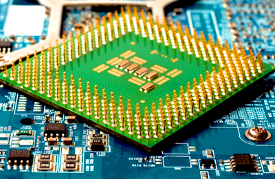
Physical Design & Sign Off
Advanced geometry nodes 5nm, 7nm, 10nm, 14nm, 16nm expertise
Implementation experience for various foundries – Samsung, TSMC, Intel, etc.
Flow and methodology development for PNR, STA, PV and RV flows
Low power design implementation of advanced technologies (UPF based flows)
Block and subsystem level Physical design – CPU, GPU, High Speed Wireless LAN, ARM core
Bump planning for 2D, 2.5D and 3D ASIC stacking
CHIP area reduction and MFU optimization
STA sign-off with AOCV and POCV
Physical Verification of ASIC and blocks
RV(EM/IR), FV and Low-power checks